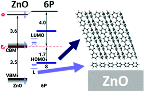
Fermi Energy Level In Semiconductor - Fermi Level An Overview Sciencedirect Topics : Above is a diagram (ref.
byAdmin-
0
Fermi Energy Level In Semiconductor - Fermi Level An Overview Sciencedirect Topics : Above is a diagram (ref.. Conduction band edge to vacuum ref. (a) holes (b) electrons (c) ions (d) all the above. An intrinsic semiconductor is (a) free electron free The fermi energy is an energy difference (usually corresponding to a kinetic energy), whereas the fermi level is a total energy level including kinetic energy and potential energy. In a perfect semiconductor (in the absence of impurities/dopants), the fermi level lies close to the middle of the band gap 1.
Fermi energy of an intrinsic semiconductor from lampx.tugraz.at the fermi energy or level itself is defined as that location where the probabilty of finding an occupied state (should a state exist) is equal to 1/2, that's all it is. The filled energy level closest to the top of an energy level diagram for a semiconductor is called the valence band. The fermi energy is only defined at absolute zero, while the fermi level is defined for any temperature. The fermi level lies between the valence band and conduction band because at absolute zero temperature the electrons are all in the lowest energy state. For the intrinsic semiconductor at 0k,
Energy Level Alignment At Organic Inorganic Semiconductor Heterojunctions Fermi Level Pinning At The Molecular Interlayer With A Reduced Energy Gap Physical Chemistry Chemical Physics Rsc Publishing from pubs.rsc.org Do the intrinsic fermi energy level changes with the addition of dopants and acceptors? The density of electrons in the conduction band equals the density of holes in the valence band. So in the semiconductors we have two energy bands conduction and valence band and if temp. Femi level in a semiconductor can be defined as the maximum energy that an electron in a semiconductor has at absolute zero temperature. Fermi levelis the state for which there is a 50% probability of occupation. Green, unsw) illustrating the location of the fermi level ef relative to the valence and conduction bands for various materials. The intrinsic fermi energy level always remains constant because it is an imaginary level taken to distinguish between the fermi level of the types of semiconductor. This definition of fermi energy is valid only for the system in which electrons are free (metals or superconductor), or any system.
I.e., different materials will have different fermi levels and corresponding fermi energy.
The fermi level plays an important role in the band theory of solids. Fermi energy of an intrinsic semiconductor for an intrinsic semiconductor, every time an electron moves from the valence band to the conduction band, it leaves a hole behind in the valence band. When calculating how many electrons will fill these levels and thus be counted in n, contributing to The fermi level lies between the valence band and conduction band because at absolute zero temperature the electrons are all in the lowest energy state. The intrinsic fermi energy level always remains constant because it is an imaginary level taken to distinguish between the fermi level of the types of semiconductor. Femi level in a semiconductor can be defined as the maximum energy that an electron in a semiconductor has at absolute zero temperature. The fermi level is the surface of fermi sea at absolute zero where no electrons will have enough energy to rise above the surface. Fermi energy of an intrinsic semiconductor from lampx.tugraz.at the fermi energy or level itself is defined as that location where the probabilty of finding an occupied state (should a state exist) is equal to 1/2, that's all it is. In a perfect semiconductor (in the absence of impurities/dopants), the fermi level lies close to the middle of the band gap 1. In metals and semimetals the fermi level ef lies inside at least one band. The filled energy level closest to the top of an energy level diagram for a semiconductor is called the valence band. Fermi energyis the difference highest occupied state and lowest occupied state at 0k. However, in semiconductors the bands are near enough to the fermi level to be thermally populated with electrons or holes.
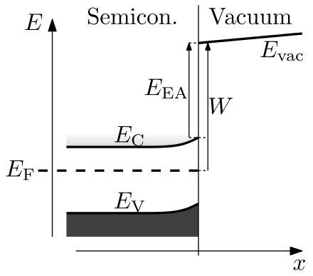
It is important in determining the electrical and thermal properties of solids. An intrinsic semiconductor is (a) free electron free The density of electrons in the conduction band equals the density of holes in the valence band. Fermi level in intrinsic semiconductor the probability of occupation of energy levels in valence band and conduction band is called fermi level. The energy gap e g, also called the bandgap, is the energy difference from the top of the valence band to the bottom of the conduction band.
Work Function Wikiwand from upload.wikimedia.org The fermi level is the surface of fermi sea at absolute zero where no electrons will have enough energy to rise above the surface. In the hypothetical case that the effective mass of electrons and the effective mass of holes are equal, the fermi level of a perfect intrinsic semiconductor would be at the center of the band gap. In metals and semimetals the fermi level ef lies inside at least one band. The energy gap e g, also called the bandgap, is the energy difference from the top of the valence band to the bottom of the conduction band. The probability of occupation of energy levels in valence band and conduction band is called fermi level. The occupancy f (e) of an energy level of energy e at an absolute temperature t in kelvins is given by: The fermi level and fermi energy will be changing depending on the type of material. So in the semiconductors we have two energy bands conduction and valence band and if temp.
Above is a diagram (ref.
Green, unsw) illustrating the location of the fermi level ef relative to the valence and conduction bands for various materials. An intrinsic semiconductor is (a) free electron free The fermi level and fermi energy will be changing depending on the type of material. The fermi level is referred to as the electron chemical potential in other contexts. Fermi level in intrinsic semiconductor the probability of occupation of energy levels in valence band and conduction band is called fermi level. The fermi energy is an energy difference (usually corresponding to a kinetic energy), whereas the fermi level is a total energy level including kinetic energy and potential energy. The fermi level is the surface of fermi sea at absolute zero where no electrons will have enough energy to rise above the surface. The intrinsic fermi energy level always remains constant because it is an imaginary level taken to distinguish between the fermi level of the types of semiconductor. In a perfect semiconductor (in the absence of impurities/dopants), the fermi level lies close to the middle of the band gap 1. The occupancy f (e) of an energy level of energy e at an absolute temperature t in kelvins is given by: The fermi level is the energy level which is occupied by the electron orbital at temperature equals 0 k. When calculating how many electrons will fill these levels and thus be counted in n, contributing to In metals and semimetals the fermi level ef lies inside at least one band.
In a semiconductor, the fermi level is indeed in the forbidden band, however there are no available states in the forbidden band. In a perfect semiconductor (in the absence of impurities/dopants), the fermi level lies close to the middle of the band gap 1. Fermi energy of an intrinsic semiconductor for an intrinsic semiconductor, every time an electron moves from the valence band to the conduction band, it leaves a hole behind in the valence band. The fermi energy is only defined at absolute zero, while the fermi level is defined for any temperature. The highest energy level that an electron can occupy at the absolute zero temperature is known as the fermi level.
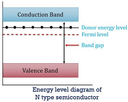
Difference Between P Type And N Type Semiconductor With Comparison Chart Electronics Desk from electronicsdesk.com Fermi energy level (a) is the top most filled energy level at 0k temperature (b) is the top most filled energy level at 00c temperature. For the intrinsic semiconductor at 0k, The density of electrons in the conduction band equals the density of holes in the valence band. The occupancy f (e) of an energy level of energy e at an absolute temperature t in kelvins is given by: This is one definition and if we apply concept of fermi level in semiconductors we say it is an energy level between the forbidden band gap (where no electron exists as per the definition) where only the probability is 50%. This definition of fermi energy is valid only for the system in which electrons are free (metals or superconductor), or any system. It is important in determining the electrical and thermal properties of solids. I.e., different materials will have different fermi levels and corresponding fermi energy.
The fermi energy is an energy difference (usually corresponding to a kinetic energy), whereas the fermi level is a total energy level including kinetic energy and potential energy.
Why is fermi level important? In a perfect semiconductor (in the absence of impurities/dopants), the fermi level lies close to the middle of the band gap 1. The fermi level plays an important role in the band theory of solids. The fermi level is the surface of fermi sea at absolute zero where no electrons will have enough energy to rise above the surface. The highest energy level that an electron can occupy at the absolute zero temperature is known as the fermi level. The energy gap e g, also called the bandgap, is the energy difference from the top of the valence band to the bottom of the conduction band. The concept of fermi level and the fermi energy are the most important topics to be studied in semiconductor physics to attain a detailed understanding regarding band. In the hypothetical case that the effective mass of electrons and the effective mass of holes are equal, the fermi level of a perfect intrinsic semiconductor would be at the center of the band gap. Semiconductor doping and higher temperatures can greatly improve the conductivity of the pure semiconductor material. Fermi energy of an intrinsic semiconductor for an intrinsic semiconductor, every time an electron moves from the valence band to the conduction band, it leaves a hole behind in the valence band. The fermi energy is only defined at absolute zero, while the fermi level is defined for any temperature. In metals and semimetals the fermi level ef lies inside at least one band. For si withnd= 1015 cm3andni = 1010 cm3, using equation 3, ef nis 0.25evaboveef i.
(a) holes (b) electrons (c) ions (d) all the above fermi level in semiconductor. In a perfect semiconductor (in the absence of impurities/dopants), the fermi level lies close to the middle of the band gap 1.